The Evolution Of Patterned Wafers: Past, Present, And Future
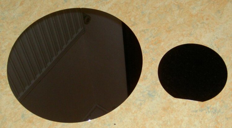
A wafer is a semiconductor material shaped like a thin disc made of silicon, one of today’s most prevalent semiconductors. Electronic integrated circuits (ICs) and silicon-based photovoltaic cells are made from wafers. This acts as the substrate in these designs. Engineers use doping, implantation, and etching to finish building the integrated circuit.
A solid “pipe” or chunk of silicon purified, melted, and cooled is the basis for using a wafer in integrated circuits. Then, it is very thinly sliced into wafers. To create n-type or p-type silicon microcells, various compounds referred to as “dopants” are employed, and techniques like sputtering, vapor deposition, and molecular beam epitaxy are utilized to remove or engrave a pattern into the wafer. This is done in clean rooms to prevent contamination and other issues linked to operating at this nanoscale.
The main idea is that different charges and substrate conditions are grouped on the tiny Test Wafers surface to enable complicated operations to be carried out on its small physical footprint. In the past, less sophisticated techniques were required (such as using vacuum tubes in the ENIAC); the invention of contemporary substrate design opens up enormous possibilities in device innovation.
The Potential Of Patterned Wafer
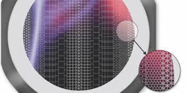
Source: corial.plasmatherm.com
They have great potential in several industries, including electronics, health, and energy. Here are some instances of what they could do:
Electronics
Patterned wafers are already utilized extensively in the semiconductor sector to create integrated circuits, but they have much more potential. They can produce more innovative semiconductors, which aligns with the rise in demand for smaller, quicker, and more potent gadgets.
Medicine
Patterned wafers could be used in the medical industry, particularly microfluidics. Constructing diagnostics, drug delivery systems, and other applications is feasible by fabricating microchannels and microstructures on a wafer.
Energy
Patterned wafers can be employed in manufacturing photovoltaic cells to make solar panels more efficient and affordable. More light can be trapped, and the solar cell’s efficiency can be raised by patterning the silicon wafer’s surface.
Optics
Optical components like lenses, filters, and diffraction gratings can be made using patterned wafers. Designing precise structures that can influence light in particular ways by patterning its surface is feasible.
A Brief History of Patterned Wafers
Source: semiengineering.com
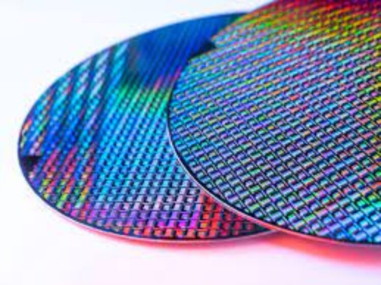
During the early stages of chip technology development in the 1950s and 1960s, basic integrated circuits (ICs) with just a few transistors and resistors were used. As chip technology advanced, complex and exact manufacturing processes were needed to produce ever-more-advanced semiconductors.
The application of photolithography, a technique that involves projecting a patterned image onto a wafer coated with a light-sensitive substance, was one significant invention that made it possible to create more sophisticated chips. This procedure enabled chip makers to produce increasingly minute parts and complex patterns on their devices.
The development of more sophisticated and complex technologies has also influenced chip design. Due to this, everything from cellphones and laptops to cutting-edge medical equipment and self-driving cars has come up. Overall, the development and the history of patterned wafers show the potential of human creativity and the value of variety and accuracy in advancing technology.
The Current State of Patterned Wafers
Source: tomshardware.com
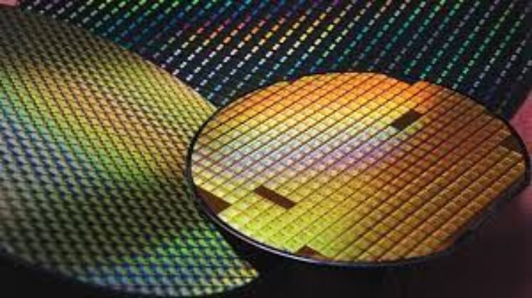
Modern chip fabrication processes and patterned wafers are closely related since they rely on cutting-edge manufacturing procedures to produce more detailed and sophisticated designs.
Current chip production processes use several methods, such as photolithography, ion implantation, and other sophisticated manufacturing techniques, to produce precise patterns and designs on silicon wafers. These methods enable the production of single-chip devices with millions or even billions of transistors and other components.
At the same time, patterned wafers have developed to include increasingly detailed and proficient patterns. Today, patterned wafers are frequently utilized in the semiconductor industry for artistic and decorative purposes and for testing and calibrating chip manufacturing equipment.
Creating cutting-edge computing and communication devices is one of the main applications of current chip technology. Modern chips are the heart of many daily devices, from smartphones and laptops to data centers and cloud computing platforms.
Modern chips are also employed in several other applications, including industrial automation, automotive systems, and medical devices. For instance, modern pacemakers, insulin pumps, self-driving cars, and factory robots require sophisticated microprocessors and sensors.
Overall, the current status of patterned wafers and modern chip production techniques illustrates how technology is still evolving and how crucial innovation and accuracy are to advancing science. These technologies will undoubtedly continue to play an essential role in determining how our world develops as they move and change.
Exploring the Future Potential of Patterned Wafers
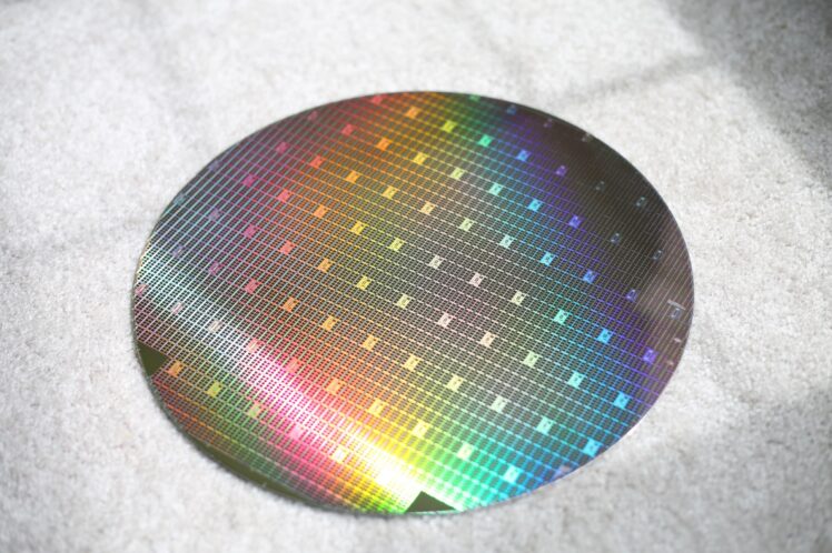
Source: electronics.stackexchange.com
Integrated chips are produced on patterned wafers, used for centuries in the semiconductor sector. However, they also have new uses in several other industries. The following are some potential uses for patterned wafers in the future:
Photovoltaics
Patterned wafers could make solar cells more efficient and affordable. More light can be trapped, raising the solar cell’s efficiency by patterning the silicon wafer’s surface.
Microfluidics
Patterned wafers could be utilized to make devices that precisely control and manipulate fluids at the microscale. Making microchannels and microscopic structures possible by patterning a wafer’s surface is possible. These can be used for various applications, including lab-on-a-chip devices, point-of-care diagnostics, and drug delivery systems.
Optics
Using patterned wafers, optical components like glasses, filtration systems, and diffraction gratings may be produced. By patterning a wafer’s surface, precise structures that can affect light in specific ways can be created.
Micro-Electromechanical Systems (Mems).
They are tiny devices that combine mechanical and electrical components and can be made using patterned wafers. Complex structures that can be used for various applications, including sensors, actuators, and microfluidic devices, can be made by patterning the surface of a wafer.
Wearable Technology
Expandable and flexible electronic components for wearable devices could be produced using patterned wafers. Circuits and sensors that can adapt to the molds of the human body can be made by patterning the surface of a wafer.
Conclusion
Patterned wafers have evolved since they were first used in the semiconductor industry. They play a crucial role in the development of electronics, computing, and telecommunications. Due to the constant demand for smaller, faster, and more potent devices, they have remained essential in creating new technologies.
Patterned wafers have a lot of potential in various cutting-edge fields like photovoltaics, microfluidics, optics, MEMS, and wearable technology. Cost, yield, and scalability are just a few of the difficulties that producers face. Due to continued technological and manufacturing improvements, they are expected to be crucial in determining the future of electronics, health, and energy.


